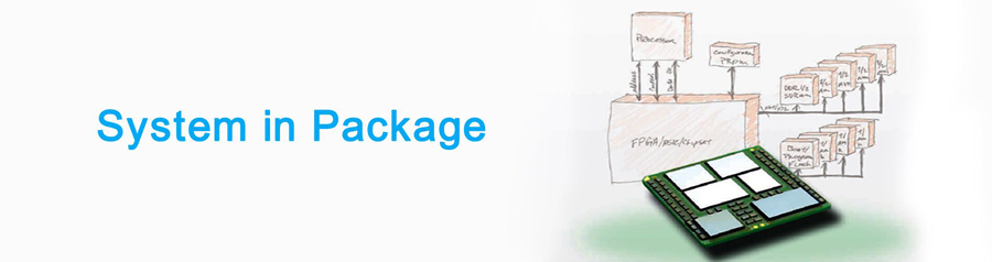
SiP is a functional system or sub-system assembled into a single package. Typically, it will contain two or more dissimilar die. For example, a FPGA, processor, data conveters and flash memories can be combined in one space-saving package.They can also be combined with other components such as sensors, triggers, passives, MEMS, voltage regulators, etc.
These are then assembled on an interposer or substrate to create a customized, integrated product for a specific application. Within the SiP, the designer can utilize bare die (wire bond or flip chip),BGA/CCGA packaged devices, stacked die or stacked packages.The benefits of this technology are:
 Greater functionality in a time-to-market window that cannot be met through silicon integration; increased density and performance. Reduced board area, weight and routing complexity at the PCB level. Board layer reduction and performance enhancements reduces PCB
costs.
Design optimization through use of the most costeffective silicon solutions and assembling different semiconductor technologies, diegeometries, or chips from different fabs in the same package.
Value added benefits include high-speed designs, assembly processes and material set incorporated into the SiP. Allows the OEM to upgrade products by using die-shrinks in the same package. Multiple techniques designed specifically for chip level anti-tamper Combining sensors, triggers and encryption to SiP products The Created common platform can be upgraded at any time,and more stable and reliable.Design for Electrical Performance
Product Development Digital, Analog, memory and RF design FPGA design (VHDL design, coding and simulation) Compact multi-output switching power supply designs Firmware Design (Embedded C, assembly and scripting languages) Experience in HDI routing and high speed design techniques Pre- and post-layout electrical simulation for PDN, crosstalk, timing and signal integrity Module Modeling EBD, IBIS, ELDO, “S” parameters
Thermal Management and Cooling of Complex Packages
Our engineers use the following techniques to insure SiP performance over the thermal environment required:
Pre- and post-layout thermal modeling to drive die position, material selection and ball arrangement Thermal vias and balls, added copper layers,enhanced seal ring and lid placement Optimized package design, component placement and material selection Electrical component characterization over target temperature extremes to establish power requirements Die and component selection with low power performance and low power operating features
Our SiP Capability
High yield flip chip assembly of wide aspect ratio die Incredible density enhancements over monolithic approach Controlled impedance, low inductance via design Density: reduced PCB layer count Reliability, Reduced part count and component I/O for better utilization of PCB routing Multiple program wins leading to volume production for use in density challenged applications Volume die utilization that leverages COTS standard silicon Offers a family of standard memory,processors,Data conveters and FPGA in BGA/CCGA packages.